|
IN
THE NEWS: Berkeley Lab's EUV Lithography
By Phillip F. Schewe, Ben Stein, And James Riordon
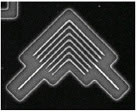
Ultraviolet
Lithography can produce lines for integrated circuits as small as
39 nm. To help sustain Moore's law and cram more and more gates
and memory units into a given space, manufacturers of microchips
must make the lines in their circuitry ever smaller. This usually
means working with a shorter-wavelength light beam for creating
the patterns used for inscribing fine features on silicon or metal
surfaces. The form of lithography currently in mass production now
can produce a half-pitch size of 90 nm and isolated line widths
of 65
nm. To produce a later generation after that you would need even
shorter wavelengths. At Berkeley Lab’s Advanced Light Source,
a government-industry consortium of scientists is trying out this
future lithography. (2/13/03) Full
story.
|