Nanosecrets of Everyday Things
|
|
|
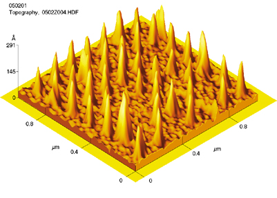
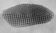
| Nanoparticle arrays of platinum crystals on a silicon oxide surface reveal the important role in catalysis played by the interface between metal and substrate. | |
Gabor Somorjai of Berkeley Lab's Materials Sciences Division, a professor of chemistry at UC Berkeley, notes that "you can increase the octane rating of gasoline remarkably" by catalyzing its hydrocarbon precursor over platinum, "but there are at least seven or eight directions the reaction can go." What's wanted are chemical structures called branched isomers, but the reaction can also can produce high-octane aromatics, which are cancer-causing molecules-or, by breaking carbon-carbon bonds, it can produce gases, "the last thing you want."
Industrial catalysts are often tiny particles of metal supported on an oxide surface, operating in a high-temperature stream of reactants. The smaller the particle, the larger the ratio of its surface to its volume; the more catalyst surface that's exposed, the more efficient the reaction.
"As long ago as the 1920s, industry began depositing metal particles on a support surface by precipitating salts from solution," says Somorjai. "The trouble is that these particles vary in size, and their spacing is random."
Size and spacing are both vital to Somorjai's goal of creating industrial catalysts with the efficiency and precision of enzymes. In collaboration with Erik Anderson and the Nanowriter facility (see page 38), Somorjai positioned single crystals of platinum 15 to 20 nanometers high just 100 nanometers apart, on a silicon oxide surface only half a centimeter square.
Tests in a high-pressure reaction cell showed that the nanoparticle array was far more selective and efficient in catalyzing reactions than platinum alone. But there was a surprise.
Between each test, Somorjai and his coworkers cleaned the catalytic array, "shaving off any organic 'dirt' by bombarding the wafer with a beam of ionized neon." The beam planed the platinum clusters down, atom by atom, until their surface area was less than half of what it had been.
Remarkably, the array remained 20 to 30 times more active than platinum alone. "It wasn't just the metal that promoted catalysis. The interface between the metal and the oxide was much more important that anyone had previously thought"-a discovery that may lead to efficient "high-tech" catalysts.
Skimming the surface
Somorjai examined his nanocrystal arrays with an atomic-force microscope, which "feels" its way across a surface. The shallows of the material world are transparent to other experimental techniques too. One is to penetrate a thin sample with a focused beam of electrons and construct an image-a kind of electronic shadow- from the interference patterns of the scattered electrons.
Often these transmission electron microscope images have a "bubble-raft" appearance, in which ordered arrays of little round blobs encounter other arrays oriented differently. Each blob represents a column of atoms; seen from a different angle, the spacing and orientation of the columns gives a different picture, although at some angles the atoms are too close together to resolve. An important challenge has been to find out how "tall" each column is-a challenge recently met at the National Center for Electron Microscopy (NCEM) by advances in computation, improved microscope hardware, and sophisticated sample preparation.
Under the direction of Michael O'Keefe and Christian Kisielowski, NCEM's One-Ångstrom Microscope (OÅM) has achieved the country's highest resolution-better than 0.8 angstrom (less than a tenth of a nanometer)-resolution so good, says Kisielowski, that "the OÅM can resolve different projections in many crystalline materials to get to the third dimension."
The OÅM makes use of "phase-scrambled" information well beyond the in-phase image components that normally define a microscope's resolution. The additional information can be deciphered by combining different images of the same sample with a computer.
Other new image-processing techniques allow individual atoms in a column of atoms to be counted, provided the atoms are heavy enough. As a result of these advances, says Kisielowski, "theory and experiment are merging. Once upon a time theorists were on their own if they designed materials on a computer. Nowadays, the atom clusters they calculate are similar in size to those we investigate, and there is a reliable way to check their predictions."
Now almost every atom in a nanocluster lying on a substrate can be accounted for. "We can, for example, locate columns of silicon atoms at a gate oxide interface-the most important interface in integrated circuit technology-with the unprecedented precision of about a hundredth of an angstrom."
The new methods are generally applicable and can visualize interfaces of different crystal, as well as lattice, defects. "Dislocations determine the plasticity of solids . . . for the first time their core structure can be examined directly in all sorts of solids," says Kisielowski. "A 20-year argument about different core models can be resolved by simply having an image with truly atomic resolution."
Flipping spins
The magnetic phenomenon of exchange bias-or "pinning"-has been known for almost half a century, but scientists at the Advanced Light Source (ALS) opened the door to a new and better understanding of the phenomenon by examining layered magnetic materials, each layer only a few nanometers thick, with the PEEM2 photoemission electron microscope.
|
|
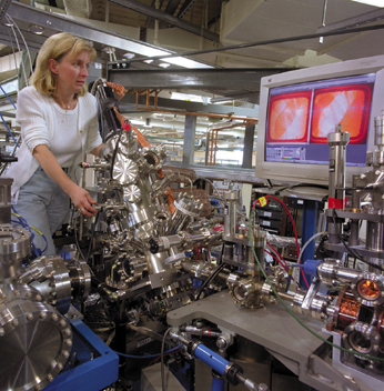 |
| Simone Anders, now at IBM, led the ALS team that built the PEEM2 microscope. Able to resolve features only tens of nanometers apart, PEEM2 has been called "the most sophisticated microscope of its type in the world." | |
Instead of penetrating the sample with an electron beam, photoemission electron microscopes and spectrometers stimulate the material to emit its own electrons-whose energy and spin convey information about elemental compositions and electronic and magnetic structures.
"A modern read head uses magnetic layers of very thin films with different properties," explains Andreas Scholl of the ALS. The magnetic structure at the interfaces of ferro- and antiferromagnetic layers determines the function of the device. "As the head passes over the hard disk, these layers sense the orientation of the domains on the disk and cause the head's electrical resistance to change in response."
The electronic spins in the magnetic domains of ferromagnets are parallel, and they all point in the same direction; ferromagnetic domains change orientation in the presence of an external magnetic field. The electronic spins in antiferromagnets are also parallel but point in opposite directions; on average, they are insensitive to external fields.
By pinning one ferromagnetic layer in a read head to an underlying antiferromagnetic layer, the other is free to respond to changing fields as the head skims over the disk. When the two ferromagnetic layers have the same orientation, they exhibit less electrical resistance than when they are opposed. Thus magnetic data on the disk is translated into variations in electric current.
To examine pinning on the nanoscale, a research team led by IBM scientists used the PEEM2 microscope on ALS beamline 7.3.1.1. When an x-ray beam hits the sample, electrons are ejected and focused into an image with 20-nanometer resolution.
 |
|
| In 1997, Portland State physicist Gertrude Rempfer demonstrated that an electron mirror could correct spherical aberration. ALS scientists have designed a more sophisticated electron mirror for the next-generation PEEM. | |
Since X-rays of different energies stimulate electrons characteristic of different elements, different layers can be viewed by tuning the energy of the beam. Magnetic domains are revealed by polarizing the beam: circular polarization produces images of ferromagnetic domains, and linear polarization shows antiferromagnetic domains.
PEEM2 images were the first to clearly show the alignment of magnetic domains in an antiferromagnetic thin film. When the researchers compared transmission electron microscope images of the same sample, they saw that the magnetic domains corresponded exactly with the orientation of the material's crystals.
Soon afterward, PEEM2 produced perfectly registered images of a ferromagnetic layer three nanometers thick overlying an antiferromagnetic layer. These showed precise correspondence between the spin orientations of the adjacent materials, domain by domain: pinning aligns the magnetic structure of both layers.
To control the orientation of the coupled ferromagnetic layer in read heads, manufacturers set a bias by annealing the multilayer devices in a magnetic field-taking advantage of the fact that magnetic materials lose their magnetism above a critical temperature but regain it when they cool.
|
|
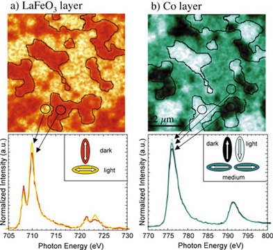 |
| Under the PEEM2 microscope, linearly polarized synchrotron x-rays show antiferromagnetic domains in a layer of lanthanum iron oxide. Corresponding ferromagnetic domains in an adjacent layer of cobalt are revealed by circularly polarized x-rays. | |
To their surprise, the researchers found that their layered test samples, although not annealed, already possessed a bias within each local domain. "Apparently exchange bias is an intrinsic property of the interface," says Frithjof Nolting, a member of the research team from Stanford University.
The discovery, he says, "opens the door to new investigations, which may affect the way devices based on the exchange bias effect are manufactured"-and the magnetic materials used to make them.
To further these researches, ALS scientists and their international colleagues are even now racing to build a third-generation PEEM that will eliminate spherical and chromatic aberration, achieving the finest possible resolution, an order of magnitude better than PEEM2's.
Into the depths
"The surface is an unavoidable defect in the crystalline structure," as science historian Ernest Braun wrote; the fundamental nanosecrets of solids lie deeper. One way to dig them out is with transmission electron microscopy.
 |
|
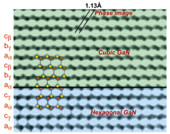
| In this image of gallium nitride, heavy gallium atoms (red) and light nitrogen atoms (green) are separated by only 1.13 angstroms. The first microscope to resolve light atoms in the presence of heavy ones was NCEM's OÅM. | |
Metallurgists have long known how to make strong alloys, even without understanding their microstructure. First heat the constituents until they dissolve in one another, then allow the alloy to "age" for several days; one or more of the constituents may precipitate out of solution and form microscopic inclusions in the matrix, forming a considerably stronger alloy. Precipitation hardening has been crucial to aviation since the first powered flight- although the Wright brothers didn't know it.
With the help of mechanic Charles Taylor, the Wrights designed and built the Flyer's 12-horsepower engine in their own shop. The 180-pound engine was wrecked after the fourth flight of the day, but a recent analysis of a long-lost piece of it showed that the Wrights made it of precipitation-hardened aluminum-copper-seven years before such alloys were knowingly used in aviation.
"Not until the last few decades have scientists been able to investigate how metallurgists achieved these effects," says Uli Dahmen, head of NCEM, "and in fact it's only now that we're beginning to get a thorough understanding of crystal structures and the interface between precipitates and the matrix."
|
|
"We've
progressed well beyond alchemy and the Wright Brothers." |
 |
The closer the spacing of precipitates, the harder the alloy. So-called S-phase inclusions in advanced alloys such as aluminum 2219, which includes copper and magnesium, are so small and constitute such a small percentage of the total composition that their crystalline structure and orientation could only be guessed. In 1999 a team including Dahmen, led by NCEM visitor Velimir Radmilovic, professor of metallurgy at the University of Belgrade, found that none of the proposed models was correct.
"To do the study we combined microscopy and computing in a fully quantitative data analysis, using every pixel in every image," says Dahmen. "Although these precipitates are only a few nanometers in size, we were able to get a clear understanding of their unique crystal structure and shape-and how they strengthen the alloy."
Using sophisticated software recently developed by NCEM's Roar Kilaas, various simulated "ideal" images were repeatedly compared to real images
of 2219 to find the best fit, thus revealing the precipitates' unknown crystal structure. The brick-shaped precipitates, themselves composed of aluminum, copper, and magnesium, form at two different angles in the pure aluminum matrix; in one orientation the edge of the "brick" has regular stepped ledges.
"The apparently odd orientation of the precipitates within the matrix allows them to make a perfect fit with the lattice structure of the matrix at the interface," says Dahmen.
Because precipitates interrupt the crystalline structure of the matrix material, they interfere with shearing. The more different orientations their own crystal structure allows, the better they can halt shearing along the matrix's crystal planes. And the thicker their dispersion, the shorter any shear that does get started.
As inclusions approach nanoscale, their thermal response also changes dramatically. "The energy of their interface with the matrix becomes more important than their internal energy," Dahmen says. Thus a nanosize inclusion may melt at a much higher or much lower temperature than the bulk material, or it may have a crystal structure that is simply not stable in particles larger than a few nanometers.
 |
|
| At a grain boundary in aluminum, transmission electron microscopy shows different interfaces among facets of a precipitate crystal in atomic detail. | |
Applying their new knowledge, Radmilovic, Dahmen, and their colleagues have patented a new alloy of aluminum, copper, germanium, and silicon for use in the aerospace and automotive industries. The new alloy is characterized by an extremely dense distribution of ultrafine precipitates of two different compositions, one kind piggybacking on the other. Harder and more stable than 2219, the new alloy is also more energy-efficient to manufacture and apply.
"Scientific investigation of nanoscale inclusions in solids is not
always recognized as 'nanoscience,'" says Dahmen. "That may
be because metallurgists were so successful for so long at developing
better materials without the help of a scientific understanding. But that
situation is changing rapidly. By probing the atomic structure of materials
with electron microscopy, we are learning how their properties can be
controlled on the nanoscale. We've progressed well beyond alchemy and
the Wright brothers."
-
end -
| < Research Review | Top ^ | Next > |