SHAPING THE WORLD ATOM BY ATOM
|
|
|
 |
|
 |
|
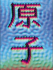
| Reading, Writing and Arithmetic. (top) A computer
read-head works by passing over layers of very thin films-a few nanometers
thick- with differing magnetic properties. As the layers sense the
orientation of the magnetic properties, the head's electrical resistance
changes. (Middle) Written literally with atoms, the Japanese Kanjii
pictured-just a few nanometers across-means "atom." (Bottom)
In the world's smallest abacus, molecules represent the numbers from
zero to ten. The "beads,"-atoms of C60-are moved along steps
just one atom high using the tip of a scanning tunneling microscope. Image courtesy IBM corp. |
|

In its broadest definition, "nanotechnology" refers to the construction and use of structures and devices that range in size from one to 100 nanometers, a nanometer being one billionth of a meter. How small is this? A dot one nanometer in diameter would be approximately 100,000 times smaller than the diameter of a human hair. A typical virus measures 100 nanometers across. Nanometer-sized features on a computer chip would be about a thousand times smaller than the micrometer-sized features on today's chips. This would mean that all the information stored in the Library of Congress could be contained in a computer the size of a sugar cube. By today's standards, that's a supercomputer that can fit in the palm of your hand.
The arrival of the nano-age will mean that humans can process matter on a molecular scale; that is, we will be able to build things atom by atom or molecule by molecule.
When construction takes place at the molecular level, there is virtually no limit to the shape and size of the objects and devices you can make. The nano-age is coming, but how soon this technology arrives will depend upon scientific research.
"If the dream of molecular-scale matter processing is to become a reality, it will require research on structures of nanometer dimensions, and their assembly into complex functional systems, that is integrated across a broad range of disciplines," says physicist Daniel Chemla, director of both the Materials Sciences Division (MSD) and the Advanced Light Source (ALS) at Berkeley Lab and a leading authority on the optical and electronic properties of nanoscale materials.
Chemla, like many other leaders in the materials sciences, advocates changing the paradigm for nanotechnology research by reducing the time that elapses between the design, synthesis, measurement and analysis of new materials.
"The ultimate goal is to give the U.S. high-tech industry all the tools it will need to make new molecules and nano-sized objects," he says.
Berkeley Lab is well poised to help the nation advance toward this goal. Its nanoscience program was begun under Chemla's direction over a decade ago, before the field was recognized as an important area of research.
"We reoriented research activities at MSD's major facilities-the National Center for Electron Microscopy and the Center for X-Ray Optics-to the study of structures of nanoscale dimensions," Chemla says. "More than two dozen division investigators were encouraged to expand their research programs to encompass the field. We also collaborated with the University of California at Berkeley Departments of Physics, Chemistry, and Materials Sciences to recruit many top young scientists, and then provided them with start-up funds from Berkeley Lab's own Laboratory Directed Research and Development Program to help them establish nanoscience programs."
Research at Berkely Lab already encompasses "hard" (inorganic) materials, including nanocrystals, nanotubes, and lithographically patterned structures, and "soft" (organic and living) materials, such as polymers, DNA, proteins, and components of living cells. The nanometer scale is the dimensional regime where hard and soft materials sciences meet, and Lab researchers already invoke the primary fabrication strategies of both: the "top-down" approach practiced by solid-state physicists and physical chemists in which existing structures and objects, such as semiconductors, are made smaller; and the "bottom-up" approach practiced by chemists and molecular biologists in which atoms and molecules are connected together to make larger structures and objects.
"For hundreds of millions of years, nature has assembled proteins and other biological molecules to build a variety of molecular machines," explains Chemla. "The living cell is the ultimate example of nanoscale matter-processing."
|
|
"The living cell is the ultimate example of nanoscale matter- processing." |
In addition to well-established and strong programs in materials sciences, Berkeley Lab also hosts three national user facilities that offer cutting-edge technical capabilities crucial to effective nanoscale research-the ALS, a synchrotron radiation source that generates some of the brightest and most intense x-rays available for scientific research; the National Center for Electron Microscopy (NCEM), where researchers can "see" atoms in a crystal and have achieved subangstrom resolutions of structural details; and the National Energy Research Scientific Computing Center (NERSC), which is one of the most powerful unclassified computing resources in the world.
The ability of the microscopes at NCEM to resolve images of objects at the atomic level speaks for itself, but the ALS gives researchers here an added dynamic. It is not enough merely to "assemble" nanoscale objects and view them, researchers will also need to observe them in action to evaluate their performance. This means studying how the various properties of a given object may evolve over a period of time under changing conditions. Given the size of the object being studied, these time periods can be astonishingly short. For example, observing the dynamics of a microchip's electronic properties may require making measurements within a few billionths of a second. Observing the same dynamics in a nanometer-sized semiconductor can require time measurements a million times more brief. This is called the "femtosecond" scale: a femtosecond is to one second what one second is to 30,000 years. The ALS, which routinely delivers strobes of x-rays in picosecond pulses (trillionths of a second), has recently been rigged to yield femtosecond timescale flashes as well.
In addition to experimentation, nanoresearch also requires a substantial amount of theoretical modeling. For this work, the brute computational power provided by NERSC becomes a necessity. Theoretical models of hard materials in the past have yielded useful predictions based on the description of only a few atoms arrayed in a crystal, thanks to the periodic structure of crystals. Nanosized structures and objects will be an entirely different story. These constructs might require the modeling of millions of atoms which may be arranged in a very precise order but without the periodic symmetry of a conventional crystal. NERSC is one of the few places on the planet with the capabilities to handle number-crunching of this magnitude.
Berkeley Lab, with its unique combination of national user facilities and strong research programs in the materials sciences, is an ideal location from which to begin a change in the nanotechnology research paradigm, as Chemla explains.
"Such a change calls for the kinds of multidisciplinary programs across condensed matter physics, physical chemistry, organic chemistry, materials sciences, biology, and ultrasmall device physics already present at Berkeley Lab. Furthermore, at Berkeley Lab, we can provide researchers with instrumentation and equipment that is too expensive, too infrequently used, and too demanding of technical staff to be generally available in university or industrial laboratories. We also offer some of the best characterization facilities in the country."
|
|
|
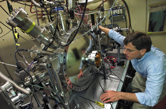
| Robert Schoenlein, a physicist with Berkeley Lab's Materials Sciences Division, was a member of the team that extracted femtosecond-scale pulses of light directly from the electron beam of the Advanced Light Source-a technological first. | |
The characterization facilities to which Chemla refers include the existing Center for X-ray Optics and its unique electron-beam nanowriter plus a new, one-of-its-kind nanofabrication laboratory now in the planning stage that will provide state-of-the-art lithography and thin-film processing.
Unlike the microlabs of today, where standardized equipment and facilities are used to create standardized devices and structures for specific functions at ever-smaller scales, the proposed nanofabrication laboratory would be dedicated to the multifunctional processes and techniques most directly relevant to chemical and biological nanosystems. Instead of processing electrons and photons, researchers at the new nanofabrication laboratory would truly be able to process matter itself.
"Working at the nanometer scale is not simply doing micron-level work with smaller objects," says Chemla. "Matter at the nanometer scale exhibits very special properties because of quantum size effects, altered thermodynamics, and modified chemical reactivity. Under our vision for Berkeley Lab, we would have the facilities and the scientific staff to meet this much greater challenge."
| < Research Review | Top ^ | Next > |