|
|
| |
 |
 |
|
| |
 |
| |
|
| |
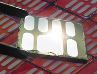
Above: Chemist Paul Alivisatos, director
of Berkeley Lab's Molecular Foundry, in his laboratory
where he and his team developed a hybrid semiconductor
and plastic solar cell (top). The tiny solar cell assemblies
were created using nanoscale rods of cadmium selenide
and the P3HT polymer. Such cells will be cheaper and easier
to make than their semiconductor counterparts. |
| |
|
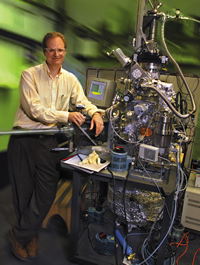
The hybrid solar cells were developed by Paul Alivisatos,
a chemist who holds a joint appointment with Berkeley Lab's
Materials Science Division (MSD) and UC Berkeley's Chemistry
Department, along with Janke Dittmer, an MSD staff scientist,
and UC Berkeley graduate student Wendy Huynh. The researchers
believe their hybrid cell will be cheaper and easier to make
than its semiconductor counterparts and offer the same nearly
infinite variety of shapes as pure polymers.
"We have demonstrated that semiconductor nanorods can
be used to fabricate readily processed and energy-efficient
hybrid solar cells together with polymers," says Alivisatos,
director of the Molecular Foundry, a center for nanoscience
now being established at Berkeley Lab.
At the heart of all photovoltaic devices are two separate
layers of materials, one with an abundance of electrons that
functions as a "negative pole," and one with an
abundance of electron holes (vacant, positively-charged energy
spaces) that functions as a "positive pole." When
photons from the sun or some other light source are absorbed,
their energy is transferred to the extra electrons in the
negative pole, causing them to flow to the positive pole and
creating new holes that start flowing to the negative pole.
This electrical current can then be used to power electronic
devices.
In a typical semiconductor solar cell, the two poles are
made from n-type and p-type semiconductors. In a plastic solar
cell, they're made from hole-acceptor and electron-acceptor
polymers. In their new hybrid solar cell, Alivisatos and his
colleagues used the semicrystalline polymer known as poly(3-hexylthiophene)
or P3HT for the hole acceptor or negative pole, and nanometer-sized
cadmium selenide (CdSe) rods as the positive pole.
"With CdSe rods measuring 7 by 60 nanometers, our hybrid
solar cells achieved a monochromatic power conversion efficiency
of 6.9 percent, one of the highest ever reported for a plastic
photovoltaic device," says Alivisatos.
Even so, Alivisatos says that many engineering tricks can
be applied to make future versions of the hybrid solar cells
much more efficient.
Growing Striped Nanowires
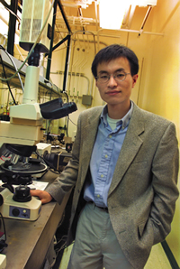
Development of nanowires composed of two different semiconductors
was led by Peidong Yang, a chemist who also holds a joint
appointment with Berkeley Lab's Materials Sciences Division
and UC Berkeley's Chemistry Department. These nanowires are
called "striped" or "superlatticed" because
their semiconductors (silicon and a silicon/germanium alloy)
are arranged in discrete alternating segments. They have potential
because they can function as a transistor, light-emitting
diode, biochemical sensor, heat-pumping thermoelectric device,
or all of the above, along the same length of wire.
|
|
 |
|
| |
|
 |
|
| |
|
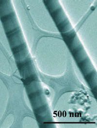
Above: Chemist Peidong
Yang led the development of a new "striped"
nanowire.
The image at top, taken with a scanning transmission electron
microscope, reveals two nanowires featuring alternating
bands of silicon (light) and a silicon germanium alloy
(dark), which form interfaces that could be made into
transistors, LEDs, and other types of electronic devices.
Each wire is less than a hundredth the diameter of a human
hair. |
|
|
|
"This is a major advancement in the field of one-dimensional
nanostructure research," says Yang. "It gives us
the ability to create various functional devices, such as
a p-n junction, a coupled quantum dot structure, or a bipolar
transistor, on a single nanowire--which can then be used as
a building block for constructing more complex systems."
Microchips have been likened to sandwiches in that they are
made by depositing layers of different types of semiconductors
with different electrical properties on a wafer of silicon.
The interfaces between these different layers control the
flow of electrons and enable transistors and other electronic
components to function. Striped nanowires offer the same electronic
diversity as a two-dimensional microchip in a one-dimensional
nanoscale platform.
Yang and his research team grow their striped wires using
a hybrid "pulsed laser ablation/chemical vapor deposition"
process. A silicon wafer coated with a thin layer of gold
is heated in a furnace so that the gold film forms a liquid
alloy with the silicon and spontaneously breaks up into nanometer-sized
droplets. Vapors of the two semiconductors will then condense
around the gold droplets as deposits which become nanowire
segments. Chemicals are used as the source of the silicon
vapor and a laser is used to vaporize the germanium. When
the laser is off, only silicon is deposited on the gold particles;
when the laser is on, both silicon and germanium are deposited.
"By periodically turning the laser on and off--and this
can be readily programmed--we can form a silicon and silicon/germanium
superlattice on every individual nanowire in a block-by-block
fashion," says Yang. "The entire growth process
resembles the living polymerization synthesis of a block copolymer."
The technique is efficient and cheap. In just one hour, millions
of striped nanowires can be made at relatively small cost.
Working with Yang on the striped nanowire project were UC
Berkeley graduate students Yiying Wu and Rong Fan.
-- Lynn Yarris
|