hese days a chip the size of a postage stamp can hold millions of electronic components; to pack in more, the features must be made even smaller. Pursuing this goal is an important objective of the Center for X-Ray Optics (CXRO), headed by David Attwood. Using an extreme-ultraviolet interferometer built and operated at the Advanced Light Source, the Center's researchers are measuring optical systems to within a fraction of a nanometer.
Integrated circuits are etched on semiconductor wafers after a camera projects a reduced image of the circuit diagram onto them. The fundamental limitation to feature size in this optical printing process is the wavelength of the illuminating light, and when it comes to visible light, "We're on the verge of a hard limit," says Jeffrey Bokor, principal investigator for CXRO's extreme-ultraviolet interferometry project. "Three or four promising technologies have been proposed, but there are no clear winners," Bokor says. "Right now it's a horse race."
|
(Click on image to enlarge)
|
|
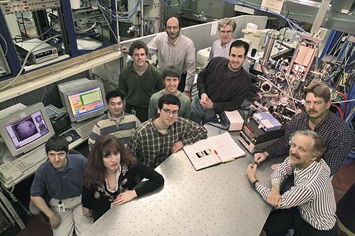
The CXRO research team.
|
The horse the CXRO group is backing involves lithography cameras using the short wavelengths of extreme ultraviolet light (EUV), which could produce circuit features no wider than a ten-millionth of a meter. But there's a catch: EUV is readily absorbed by glass and other solids. It can't be focused through conventional lenses and can't be reflected at normal angles from ordinary mirrors.
The solution is to use special curved mirrors coated with forty or more alternating layers of two materials with very different properties for EUV light, each layer only a few atoms thick. A small amount of light is reflected from each interface between the layers and adds up constructively to form a strong reflection.
To do their job, such mirrors must be shaped to exquisite tolerances and have almost perfectly smooth surfaces. Moreover, the thickness of each layer of coating must be consistent to within the span of a few atoms.
"The scale of engineering tolerance is set by the wavelength," Bokor says. "An ordinary good 35mm camera is built to tolerances of, say, a tenth of a wavelength of 500-nanometer light. For EUV lithography, we need tolerances of a fiftieth of 13 nanometers" -- about the radius of a single atom.
CXRO developed an interferometer especially to evaluate the performance of optical systems at such exquisite tolerances; it measures optical mirror systems in the same way they are made to be used -- with EUV light.
"There are no lasers which operate at 13 nanometers," Bokor says, "but the EUV light from the undulators on the ALS is the next best thing" -- laserlike in that it is partially coherent, with all waves in step. By collimating the beam and passing it through a pinhole filter, the incoherent portion is eliminated.
Using a diffraction grating, this beam is split into two or more beams. One of these, the reference beam, is filtered of any imperfections introduced by the optical system. A second beam, the test beam, is left unchanged. Both beams fall on a charge-coupled device, where they overlap to form an interferogram.
| Lead scientists on this project
|
|
|
|
|
|
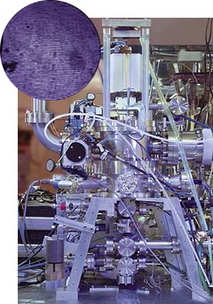
The interference pattern reveals the difference between the two beams. While a perfect optical system would produce an undistorted test beam and perfectly straight fringe patterns, real-world optics usually fall short of the mark. The subtle curvature in the fringes and the illumination pattern both reveal critical information about the test optical system unavailable to other measurement techniques. The accuracy of this novel technique has been verified to less than one angstrom (one ten-billionth of a meter) for EUV light.
In the spring of 1997, the CXRO research team -- scientists and engineers from Berkeley Lab working with a number of graduate students from UC Berkeley -- completed testing of a prototype EUV optical system designed for lithography. The optics were good but not perfect, and when the system was used to print 0.1 micron test patterns in a wafer, the performance verified the predictions from the interferometer almost exactly.
Its potential confirmed by CXRO's test interferometer, extreme-ultraviolet lithography is a horse that's still in the race for the best way of keeping up with Moore's inexorable Law.
- Paul Preuss