

| 
| 
| 
| 
|

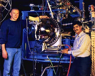
| Charles Fadley (left) and Zahid Hussain have put together what may be the world's most extensive surface science experimental station at Berkeley Lab's Advanced Light Source. Being able to characterize surfaces and interfaces of new materials will be a major advantage in the quest to fabricate the next generation of nanoscale semiconductors and magnetic storage devices. |
 Research is already under way at the MDI with first-year results that made
the cover of Science magazine. First, Berkeley Lab scientists at the institute
announced that they had found a way to deposit thousands of distinct combinations
of metal-oxide molecules onto an area the size of a checkerboard square, thereby
creating the first "combinatorial" library of advanced materials. By increasing
the number of compounds that can be created and tested as potential new materials
from about one a day to as many as 10,000 a day, this new technique, called
"combinatorial synthesis," promised to speed the pace of discovery in materials
science. This promise was vividly realized within four months of the first
announcement, when the same team of Berkeley Lab scientists announced the
discovery of a new family of magnetoresistive (MR) compounds, materials whose
electrical conductivity changes in a magnetic field.
 In recent years, new advanced materials have usually been discovered through
the substitution or altering of the ratio of atoms in a known compound (sometimes
based on the predictions of computer models). With combinatorial synthesis, in
which thousands of distinct combinations of molecules are deposited onto a square
grid the size of a checkerboard square, scientists can look at many atom
substitutions and ratio adjustments in a single combinatorial library. To look
for new materials with magnetoresistance, Berkeley Lab scientists started with a
well-studied class of MR materials based on manganese oxide, substituted similar
elements from the periodic table (iron, vanadium and cobalt) for manganese, and
made a separate combinatorial library for each one. Their cobalt oxide library
yielded 26 new materials that displayed magnetoresistance comparable to the
so-called "colossal" class of magnetoresistance materials.
 Because colossal magnetoresistant materials (CMR) become superconducting in
the presence of a sufficiently strong magnetic field, thin films of these
materials are in great demand by the electronics industry. Currently, these
materials are limited to laboratory studies, where they are made through a costly
technique called pulsed laser ablation. The situation may soon change, however.
Berkeley Lab scientists at NCEM this past year unveiled a relatively inexpensive
chemical process for making CMR thin films out of the same class of ceramic
materials that exhibit high-temperature superconductivity. At a fraction of the
cost of pulsed laser ablation, this new process holds potential for commercial as
well as scientific applications. Upon viewing their new thin films through the
powerful transmission electron microscopes at NCEM, the Berkeley Lab scientists
found they could easily vary the composition and structure in order to make a
variety of different products, including multilayer films with alternating
magnetic layers.

| 
| 
| 
|