
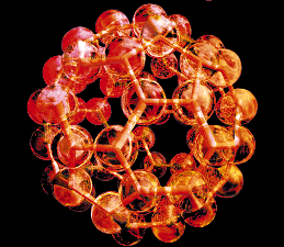
 Buckyballs are soccerball-shaped 60-atom clusters of pure
carbon that LBL scientists are using to make the world's strongest wire.
Buckyballs are soccerball-shaped 60-atom clusters of pure
carbon that LBL scientists are using to make the world's strongest wire.
Material can be made to take many forms. Solid, liquid, and gas are the most
familiar and have traditionally been the most important. However, as we move
into the next century, newer forms of materials will become increasingly
prominent. One of the most useful of these new forms of materials is thin-film.
Thin films are materials that may be no more than a single layer of atoms or molecules in thickness. Originally developed as coatings for possible use in the electronics industry, scientists are finding creative new ways to put them to use. At LBL's Center for Advanced Materials, one group has been developing thin-films for the detection of biological pathogens and environmental toxins. This past year they succeeded in making a thin-film that changes color--from blue to red--in the presence of influenza. The idea is that the film could serve as the basis of a quick and simple nasal or throat swab test for the flu virus that could be performed in a doctor's office or at the site of a possible outbreak.
Another novel form that materials can take is that of clusters--aggregates of atoms packed into spherically shaped clumps of matter that serve as a bridge between gases and bulk phase materials (liquids and solids). Too large to be thought of as a molecule but too small to be classified as a liquid or a solid, clusters frequently exhibit extraordinary properties that scientists hope to exploit in a broad number of areas. At LBL, one team has succeeded in synthesizing clusters of the semiconductor gallium arsenide into nanocrystals--crystalline particles that are a billionth of a meter, or a few angstroms, in diameter. Gallium arsenide has long been coveted by the semiconductor industry because, unlike silicon, it emits light. However, single crystals of gallium arsenide large enough to be used as a computer chip are too difficult to manufacture commercially. The goal has shifted now to creating nanocrystals of gallium arsenide for use as "quantum dots"--electronic devices a thousand times smaller than today's computer chips.
At the nano-scale level of materials, processes such as the movement of an electron across a quantum dot take place very quickly--much quicker than the blink of an eye. Studying these processes requires lightning fast new imaging instruments that can stop the action and record what happens. LBL scientists recently announced the development of new technique to do this called "ultrafast scanning probe microscopy." This new technique promises to take researchers into the domain of the picosecond--one trillionth of a second--which has heretofore been all but off-limits to microscopy.
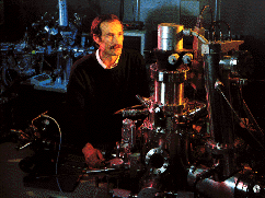 Materials scientist Miquel Salmeron and his colleagues
are using "ultrafast scanning probe microscopy" to make movies of atomic
activity on surfaces.
Materials scientist Miquel Salmeron and his colleagues
are using "ultrafast scanning probe microscopy" to make movies of atomic
activity on surfaces.
Ultrafast
scanning probe microscopy combines two cutting edge technologies: the scanning
tunneling microscope (STM), which can image details as small as a single atom;
and the short pulse laser, which can provide pulses of light that last only a
femtosecond--a millionth of a billionth of a second. Coupling these two
technologies enables scientists to record a series of time-lapse images that
can then be combined to produce a movie of surface dynamics. With this
technique, scientists hope to not only record the flow of electrons across the
surfaces of semiconductors, but also create movies of other dynamic processes,
for instance, plant photosynthesis.
Slowing the pace considerably, LBL scientists have also developed an STM that produces its images at a virtual crawl. By equipping their STM with three legs made out of a special ceramic material that bends slightly when electrified, the scientists have created a microscope that "walks" itself--a few nanometers at a time--to areas of interest on a sample. This first ever walking STM has already been used to image never-before-seen features on a gallium arsenide semiconductor. The LBL scientists also used their walking STM to produce the first images of silicon donor atoms, the electron-rich impurities that give today's computer chips special electrical properties. Whereas in previous imaging efforts, silicon donors appeared as faint shadows, in the LBL image they show up as glowing spheres. The walking STM is expected to open many new doors in materials research by making it possible for scientists in the future to study their samples atom-by-atom. This will be especially noteworthy for the semiconductor industry as it moves towards production of nano-sized electronic devices. At this small a scale, the precise placement of an individual atom in a device is critical since the size of the atom itself can set the limit of the device's performance.
No material has generated more excitement within certain circles of the scientific and industrial communities in recent years than "buckyballs." Buckminsterfullerene (the proper name) is the soccerball shaped 60-atom cluster that has joined diamond and graphite as the third known form of pure carbon. Depending on whether they are pure or doped with other atoms or molecules, buckyballs can be insulators, conductors, semiconductors, or even superconductors. For the enormous potential of buckyballs to ever be fully realized, however, they have to be made in crystalline form so that scientists can fully characterize their properties. LBL scientists have set the pace in this realm of research by successfully synthesizing and characterizing single crystals of both pure and doped buckminsterfullerene (fullerene for short). Prior to this breakthrough, characterizations of buckminsterfullerene properties had been based on granular thin films and pressed powders containing an abundance of fullerene clusters. The LBL crystallization technique has progressed so fast that this past year its creators used it to produce fullerene tubes--cylindrical crystals that are essentially one dimensional. These fullerene tubes have an even broader range of potential applications than buckyballs. For example, they could be used to make the world's strongest wire or fiber. This wire could serve as either an insulator, a conductor or a semiconductor depending on how the tubes were doped.

Return to the Table of Contents of the 1994 Regents Report